
Electroninks is one of those companies that could change the way manufacturing works. The Texas-based firm makes conductive inks, and in copper, nickel, gold, platinum, and silver, these inks can be 90% conductive while also being safer and manufacturable at scale. We previously talked to their CEO Brett Walker on the 3DPOD, and the company’s journey, from taking money from In-Q-Tel to working with FujiFilm, Scrona, and Sakata, has been going from strength to strength.
Now, the University of Texas at Austin (UT Austin) has chosen Electroninks to be a key materials supplier for its work under the Defense Advanced Research Projects Agency (DARPA) Additive Manufacturing of MicrosystEms (AMME) program. AMME‘s “ultimate goal is to demonstrate a novel, functional microsystem that integrates multiple materials within a single structure, enabling designs unattainable with conventional methods.” They want to create new materials to use for 3D printing microelectromechanical systems, or MEMS—sensors coupled with mechanical components and electronics, all made on-demand in novel, conformal, or other shapes. Essentially, they’d like to print an inertia sensor, or maybe even a hearing aid. But, of course, they can already do this, so I think AMME is, in true DARPA style, aiming a little higher, and they actually want to print your phone. I’m watching AMME like a hawk, and am super excited about this program that wishes to commercialize some truly astounding technology. After a dozen Israeli startups made it to market, the US wants to try, too.

Electroninks says that,
“AMME seeks to transform microsystem manufacturing by pioneering advancements in high-speed, high-volume, and high-resolution multi-material production. This cutting-edge additive manufacturing process will enhance commercial devices with next-generation integrated technologies while enabling rapid adaptability to evolving mission requirements—much like additive manufacturing has revolutionized complex prototyping. Through AMME, DARPA aims to break through the inherent limitations of traditional microsystem fabrication, unlocking new possibilities for innovation and scalability.”
The company will work with conductors and insulators within the same component using 3D interconnects and RDL, a redistribution layer in IC Packaging; this is a key way to connect the chip to the outside world. With 3D interconnection, several chips are placed on a wafer in a stack, saving space and increasing functionality. These are technologies that are very relevant for the most advanced devices that you use every day. The company says that, “by developing innovative conductive materials optimized for high-speed, large-area lithographic patterning, Electroninks’ contributions will help overcome fundamental limitations in current semiconductor packaging processes.”
Another way that AMME will be relevant is that it is super manufacturing-focused and meant to commercialize this technology, not just be a concept car. The company is also focusing on scalability and high-volume production, and hopes that this will lead to iterative manufacturing of electronics. Furthermore, IC packaging could become more efficient and potentially reduce energy consumption.
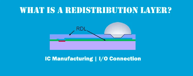
Image: Well Done Technology
As part of the AMME program, UT Austin’s Department of Mechanical Engineering is working with several industry leaders and academic institutions on innovations in semiconductor packaging. Electroninks will supply the necessary materials for AMME’s new 3D interconnection techniques. UT Austin’s Professor Michael Cullinan stated,
“AMME represents a significant step forward in semiconductor technology, addressing critical challenges in AI hardware and advanced packaging. By integrating cutting-edge materials with state-of-the-art holographic lithography, we aim to drive new levels of efficiency and capability in semiconductor manufacturing.”
Electroninks CEO Brett Walker said,
“We are obviously poised to be a significant partner for this consortium and play a key role in fulfilling DARPA’s goals. This is great news for the State of Texas, innovation and the future of technology.”
AMME could eventually change how many things are made. There are a lot of people worldwide working in IC packaging, photonics, and many related fields. But, by more efficiently connecting and building electronics, AMME could redefine how MEMS and other packages work, and how well they work. Packages could be optimized in a completely new way to be spread out, made conformal, or compacted to fit inside devices like your phone. This is a great win for Electroninks and could lead to a breakthrough in IC packaging and beyond in the years to come.
Subscribe to Our Email Newsletter
Stay up-to-date on all the latest news from the 3D printing industry and receive information and offers from third party vendors.
Upload your 3D Models and get them printed quickly and efficiently.


